


")


At the extreme edge: revolutionary sensing and display technologies
How can we cope with the ever-increasing amount of data that we generate? The answer is simple: the ‘machines’ themselves are going to help us. And that’s how we are entering an era of artificial intelligence. In this era, all internet-based applications put heavy demands on new and optimized technologies across all the layers of the digital ecosystem. At the extreme edge, we need more and more sensors – inspired by all five senses – serving the Internet of Things (IoT). In the infrastructure for the IoT, we need more quality of action – meaning faster processing, more storage and more connectivity. And finally, we need improved insights, by creating machines that can learn from the data and subsequently take action in an autonomous way. Below, I will give an overview of some of the new technology trends that imec has been working on – across all the layers of this digital ecosystem.
For a very long time, computer vision has been based on only one camera, which basically captures our 3D world into a 2D image. To recover that lost third dimension, we can make use of depth sensors. Depending on the application and range between object and sensor, different types of depth sensors are needed. For example, when we talk about very short range, fingerprint sensing comes to mind. At imec, we are developing the next-generation of fingerprint sensors, providing full display access. Two fingerprint platforms are being developed – an optical and an acoustic one. Our optical platform uses an array of organic photodiodes that can be integrated side by side with the organic LED (OLED) into the display panel and gives pixel densities up to 500ppi. The acoustic platform consists of an array of piezoelectric micromachined ultrasonic transducers (PMUTs) that is placed underneath the display. The beauty of this acoustic platform is that it can also detect cardiac pulse – as an extra measure of security.
Acoustic fingerprint sensing platform: PMUT arrays are placed underneath the full display
Moving up towards one meter range, we can think of applications such as gesture recognition. We are developing high-resolution image sensors that are sensitive to infrared light – which is safer for the human eye and creates less interference with daylight. This is possible by using thin-film photodiodes with quantum dot absorbers – able to move the wavelength from visible to infrared. Moving up further in range brings us to terahertz sensing – a technique that is extremely useful for security, environmental, agriculture or medical types of applications.
By using integrated photonics, we are developing a terahertz platform that is much more compact and power efficient than the bulky systems that are out there today.
In this era of artificial intelligence, we will also need high-quality, high resolution displays enabling applications such as augmented reality (AR). Today’s VR glasses have a pixel density of about 500 to 800ppi. In the future, besides a much higher resolution (up to 10,000ppi), we want them to be transparent, and form a natural image to the eye. And they will need user control, in a subtle, unobtrusive way. There are different ways of making AR glasses, but the techniques for semitransparent displays have one thing in common: they need a platform of high-resolution micro-OLEDs or quantum dot emitters. At imec, we are scaling down our micro-OLED platform towards higher resolution, by using 365nm lithography. With this platform, today, we can already build micro-OLEDs with a pixel density of 1250ppi, a spacing below 3µm, multicolor RGB, and a lifetime of up to 150 hours.
At the infrastructure for IoT: improved quality of action
The compute space can typically be divided into three segments. Firstly, there is the IoT sensor space, where it is all about ultralow power. For these IoT nodes, technologies based on fully depleted silicon-on-insulator (FD-SOI) are gaining ground. Secondly, there is the mobile space, where high-performance operation is desired, but heavily constrained by batteries. And thirdly, there is the high-performance space where constant power density is provided. In these high-performance nodes, the 10nm technology node is entering production, and the 7, 5, 3 and 2nm nodes will follow in the years to come.
Enabling dimensional scaling
At the 7nm node, extreme ultraviolet (EUV) lithography is one of the major process options, as it tremendously simplifies the complexity that comes along with multi-patterning immersion lithography. In recent time, tremendous progress has been made in EUV lithography, leading to improved throughput, more maturity in photoresists and resist smoothening, and innovative pellicle solutions. In the near future, we will also have to meet the challenges imposed by random defects – also called stochastic printing failures. We will do this by a combination of better materials, scanner conditions and masks, and post-development processing techniques.

Pellicle for EUV lithography
Transistor scaling: from enhancement techniques to the ultimate exploratory device
Despite the dimensional scaling that we continue to enable, transistor scaling does not happen at the .7x rate anymore for future nodes. Especially in the front-end of the transistor, gate pitch no longer scales at a .7x rate due to device parasitics. To overcome that, we increasingly make use of enhancement techniques – such as self-aligned contacts, buried power rails and fully self-aligned vias – that can for example enable metal track height scaling. But there is a downside to scaling the number of metal tracks: it also reduces the number of fins, dramatically affecting the FinFETs performance from the 3nm node onwards. That’s why imec is working on new device architectures, such as nanosheet-based transistors, and complementary FETs (cFETs). We also develop performance enhancement features, for example new metals for the contact module, and higher-mobility channel materials. And we make increasingly more use of the third dimension. We can stack nFETs on top of pFETs, or standard cells on standard cells, or analog on logic – for that, we have developed a sequential integration technique. For coarser pitches, 1 – 10µm, we can make use of wafer-to-wafer bonding techniques.
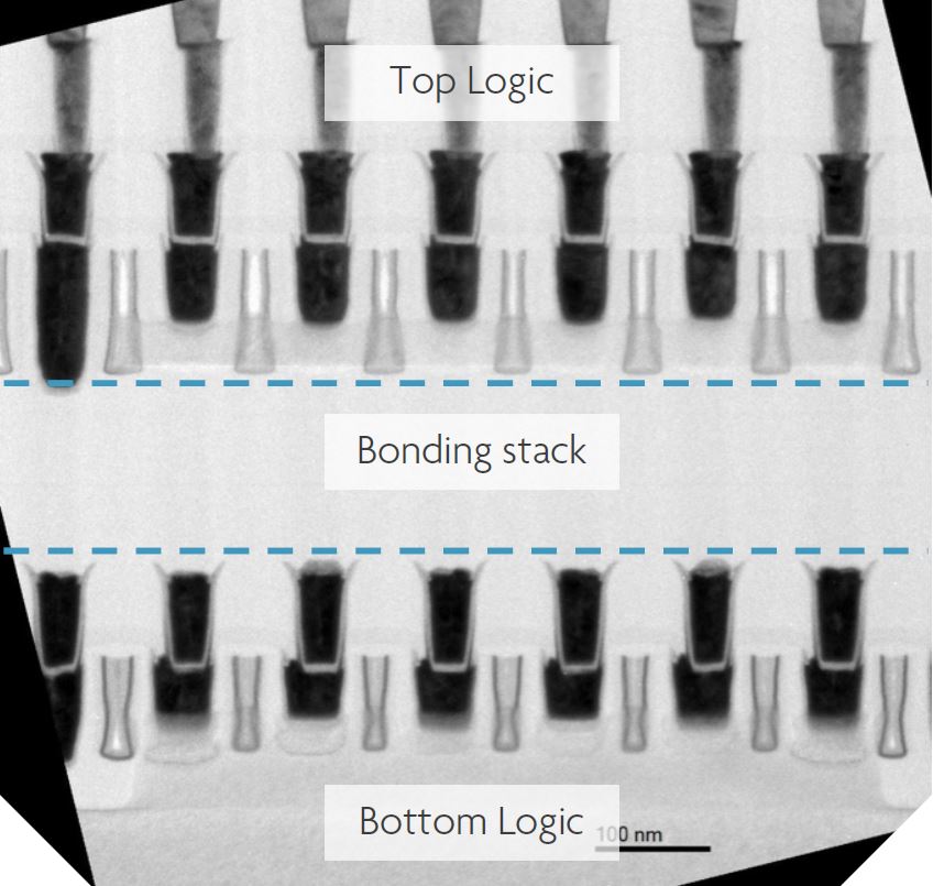
Illustration of sequential-3D integration: stacking logic block on logic block
But we also continue exploring devices that can scale beyond the charge-based CMOS transistors that we have today. In the exploratory space, a couple of devices have recently gained attention, such as the ferro-electric based devices, 2D-material based FETs, and tunnel-FETs. Imec is currently pushing these devices towards high performance to see if they can help to scale the high-performance CMOS space.
The ultimate exploratory device will make use of quantum bits – building blocks of the quantum computer. These devices promise 1000x faster calculation while consuming significantly less energy than conventional CMOS platforms.
At imec, we focus on two types of qubits – the superconducting qubit and the Si semiconducting qubit – for which we have obtained good initial results.
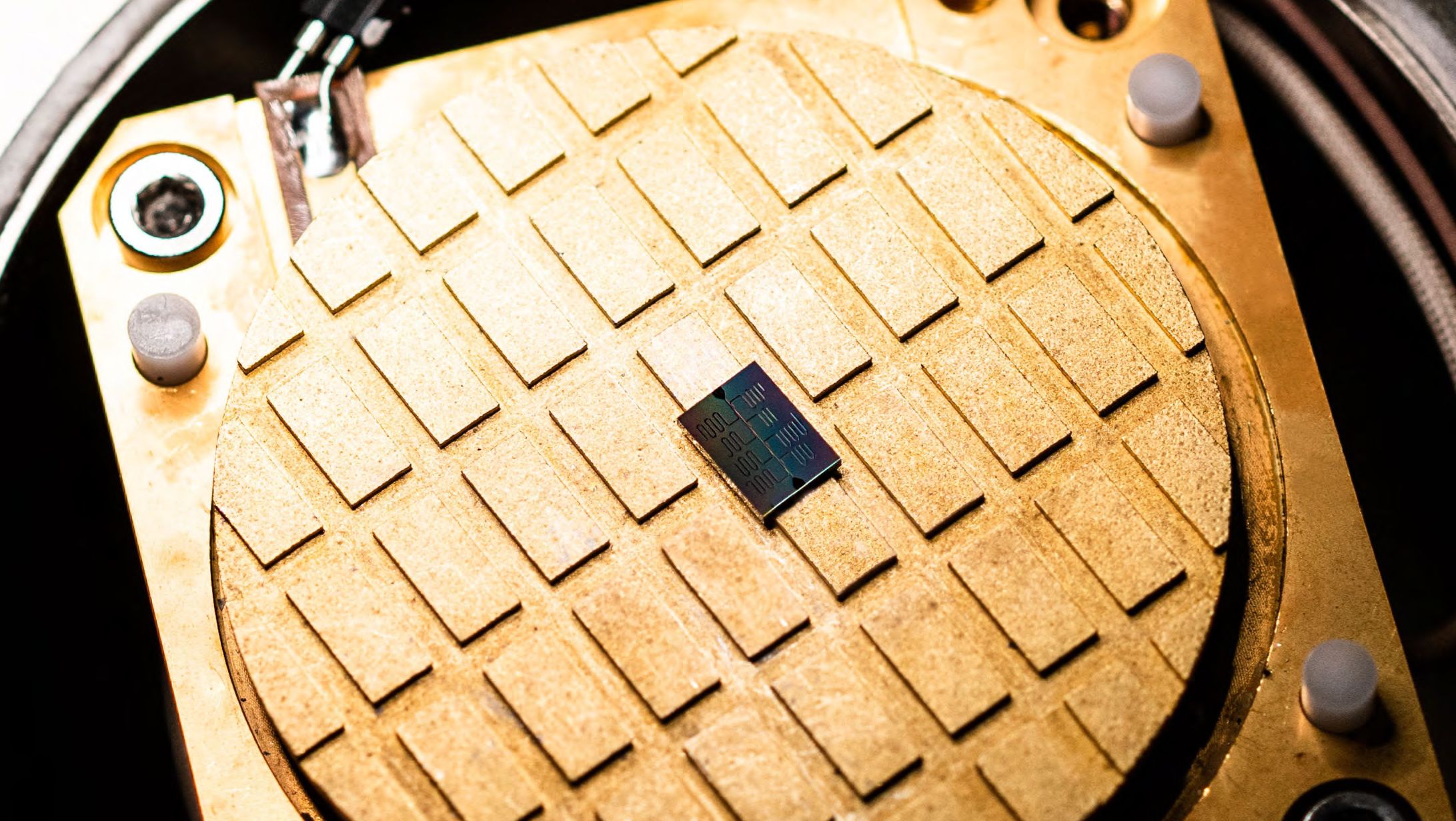
Quantum computing device
Increasing the storage capacity
If we continue to produce increasingly more data, we will also need more storage capacity. Today, our memory roadmap is under several constraints. For cheap and massive storage, we use offline hard drives; for storage on the system-on-chip, we make use of solid state Flash technology, DRAM (the ‘working memory’, which needs to be refreshed regularly) and SRAM (the ‘cache’ memory, which is volatile but faster than DRAM and more expensive). Towards the future, we expect both the NAND and DRAM space to grow. DRAM can still be scaled to smaller nodes, probably with the help of EUV lithography. And there are some new trends in the DRAM space which may boost density scaling, such as the transition from a cylinder-based capacitor architecture to a pillar-based architecture. We are also investigating if we can place logic directly under the capacitor. This requires the internal node of that capacitor to become a back-end compatible transistor.
Next, we witness a latency gap between NAND and DRAM which can be filled by storage class memory. In this context, we are proud to show the first 3D NAND type of architecture with functional ferroelectric FET devices.
And last but not least: SRAM technology is highly challenged due to the restrictions to SRAM density scaling. We have therefore been looking at new devices that can re-enable SRAM density scaling, such as our recently proposed surrounding gate transistor (in collaboration with Unisantis). Our magnetic memories are promising as well, including the spin-transfer torque magnetic random access memory (STT-MRAM) for replacing L3 cache memory, and our ultrafast spin-orbit torque MRAM (SOT-MRAM) to potentially replace L1 and L2 SRAM cache memory.
Ensuring enough bandwidth to connect the devices
So far, we have proposed solutions for fast processing all the data and store them, but we also need enough bandwidth to connect all the devices together. In the wired space, we develop solutions for both the electrical and optical space. In the electrical space, we can think of high bandwidth memory (or HBM), a high-performance interface to 3D-stacked DRAM. While state of the art HBM technology provides an aggregated bandwidth of about 2Tb/s (256 GB/s) per memory cube – which corresponds to an individual channel speed of about 2Gb/s – we are developing platforms enabling channel speeds up to 8Gb/s by using flip-chip fan-out wafer level packaging. When it comes to high performance packaging, heat dissipation becomes a true challenge. Imec recently announced a low-cost impingement-based solution for cooling chips at package level – providing designers a five times improved thermal design window compared to existing state-of-the-art cooling techniques. For data and telecom applications, optical links have become more favorable – for example to interconnect server racks in data centers or for backplane board-to-board connections. With our Si photonics platform, we develop 400Gb/s optical links (8x50Gb/s) and recently increased the performance of our platform to 1.6Tb/s to meet future needs.
And finally, in the wireless space, we anticipate the advent of 5G, which challenges the download speed of today’s CMOS based wireless devices. In the front-end of our mobile devices, we will need high-performance and high-speed analog devices with increased power efficiency. At imec, we explore a hybrid III-V/Si technology to address the 5G performance needs for the mobile space.
Machine learning for improved insights
Finally – how are we going to improve our insights? How will we make the machines themselves learn from the data and subsequently take action in an autonomous way? That’s exactly what machine learning does. Machine learning typically starts with designing a neural network that applies to the targeted application. This network is than being trained by using existing data – an action that happens in the cloud. After that, weights (which indicate the contribution of a method in a forecast) are being stored in a memory, typically off chip. Now, what happens when a new input comes in? During this deployment phase, the new input is sent to the cloud and compared to the weights. The network then gives us a probability with which this input fits in one of the classes the network has been trained for. In practice, the conventional machine learning engines typically make use of graphical processing units (GPUs) that are based on advanced CMOS technologies.
Imec is currently working on a new platform that significantly minimizes the memory requirements that come with machine learning.
It is based on (1) switching the algorithm in the deployment phase to binarization, (2) moving the non-volatile memory from off chip to on chip (compute in memory), and (3) using our 14nm technology platform with MRAM type of memories. This way, we have demonstrated a significant power reduction when compared to CMOS-based GPU technology.
With this overview, I gave a foretaste of some of the new technologies that imec is working on, and that will help shaping the world of tomorrow.
Source: https://www.imec-int.com


")